Editorial Board
Editor-in-Chief
Prof. Hongwei Zhu
Tsinghua University, Beijing, China
Research Interests: low-dimensional materials; materials informatics; carbon materials.

Co Editor-in-Chief
Prof. Xuesong Li
- 1. School of Integrated Circuit Science and Engineering (Exemplary School of Microelectronics), University of Electronic Science and Technology of China, Chengdu 611731, China.
- 2. National Key Laboratory of Electronic Thin Films and Integrated Devices, University of Electronic Science and Technology of China, Chengdu 611731, China.
- 3. Shenzhen Institute for Advanced Study, University of Electronic Science and Technology of China, Shenzhen 518110, China.
Research Interests: preparation of two-dimensional materials and new semiconductor micro-nano devices.

Editorial Board Members
Prof. Sotirios Baskoutas
Department of Materials Science, University of Patras, 26500 Patras, Greece.
Research Interests: theoretical and computational methods for the study of the electronic and optical properties of semiconductor nanomaterials; synthesis with physical methods and Characterization of amorphous and nanocrystalline materials.
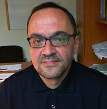
Assoc. Prof. Qiao Chen
Gemmological Institute, China University of Geosciences, Wuhan 430074, China.
Research Interests: chemical vapor deposition technology (diamond, graphene); new diamond semiconductor devices (temperature sensing, brain-like computing); gemstone optimization processing (magnetron sputtering technology, chemical vapor transport technology).

Assoc. Prof. Xuchun Gui
State Key Laboratory of Optoelectronic Materials and Technologies, School of Electronics and Information Technology, Sun Yat-Sen University, Guangzhou 510275, China.
Research Interests: two-dimensional atomic crystal materials and optoelectronic devices; flexible sensors and electronic skin; electromagnetic wave absorption and shielding devices.
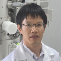
Dr. Shuai Guo
Department of Materials Science and Engineering, National University of Singapore, Singapore 117575, Singapore.
Research Interests: hygroscopic materials; hydrogels; wearable electronics; water harvesting; energy harvesting; desalination.
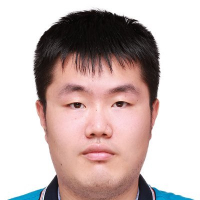
Assoc. Prof. Meirong Huang
State Key Laboratory of Photocatalysis on Energy and Environment, College of Chemistry, Fuzhou University, Fuzhou 350108, China.
Research Interests: photo(electro)catalytic water splitting; thermocatalytic ammonia synthesis.

Dr. Shiqi Huang
Department of Chemical Engineering, Centre for Integrated Materials, Processes & Structures (IMPS), University of Bath, Bath BA2 7AY, UK.
Research Interests: TP chemical technology; chemical engineering; membrane science and technology; separation; graphene; 2D materials; nanofabrication; thin films; mathematically modelling; surface science.

Assoc. Prof. Changli Li
School of Materials, Shenzhen Campus of Sun Yat-sen University, Shenzhen, Guangdong 518107, China.
Research Interests: photoelectrochemical water splitting for hydrogen production and carbon dioxide reduction using narrow bandgap semiconductors.

Assoc. Prof. Xiao Li
- 1. School of Mechanical Engineering, Jiangsu Key Laboratory for Design and Manufacture of Micro-Nano Biomedical Instruments, Southeast University, Nanjing 211189, China.
- 2. Advanced Ocean Institute of Southeast University, Nantong 226010, China.
Research Interests: sensing/energy materials; flexible wearable technology; integrated manufacturing of hydrogen fuel cell membrane electrodes.
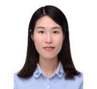
Dr. Boyang Mao
Cambridge Graphene Centre, University of Cambridge, Cambridge CB3 0FA, UK.
Research Interests: two-dimensional materials; graphene and related materials; nanomaterials synthesis; technologies for sustainable development; electrical and electronic engineering; flexible electronics.

Assoc. Prof. Fangzhu Qing
School of Integrated Circuit Science and Engineering (Exemplary School of Microelectronics), University of Electronic Science and Technology of China, Chengdu 611731, China.
Research Interests: two-dimensional heterojunction devices; applications of graphene films in electronics, optoelectronics, sensors, and other fields; preparation of large-area, high-quality graphene films.

Assist. Prof. Pengzhan Sun
Joint Key Laboratory of the Ministry of Education, Institute of Applied Physics and Materials Engineering, University of Macau, Macau 999078, China.
Research Interests: fundamental understanding of molecular transport under confinement; synthesis and processing of 2D crystals building blocks and their rationally designed assemblies for emerging technologies in environment, energy, informatics, etc.

Prof. Mingzhan Wang
Department of Materials Science and Engineering & Center of Super-Diamond andAdvanced Films (COSDAF), City University of Hong Kong, Hong Kong SAR 999077, China.
Research Interests: controlled synthesis of 2D materials; angstrom-scale nanofluidics; ion transport; membrane science and separation; energy conversion and storage.
Dr. Tingting Yang
- 1. Tribology Research Institute, School of Mechanical Engineering, Southwest Jiaotong University, Chengdu 610031, China.
- 2. Institute of Smart City and Intelligent Transportation, Southwest Jiaotong University, Chengdu 611756, China.
Research Interests: micro-nano energy devices; flexible sensors; micro-nano sensors.

Assoc. Prof. Xiaobei Zang
School of Materials and Engineering, China University of Petroleum (East China), No.66, West Changjiang Road, Huangdao District, Qingdao, 266580, China.
Research Interests: preparation and modification of new energy materials (supercapacitors, ion batteries); preparation and functional regulation of nanomaterials (graphene, metal oxides, MXene).

Prof. Tianshuo Zhao
Department of Electrical and Electronic Engineering, The University of Hong Kong, Hong Kong SAR, China.
Research Interests: nanomaterials and nanofabrication; optical and optoelectronic devices; photo(electro)chemical devices.


