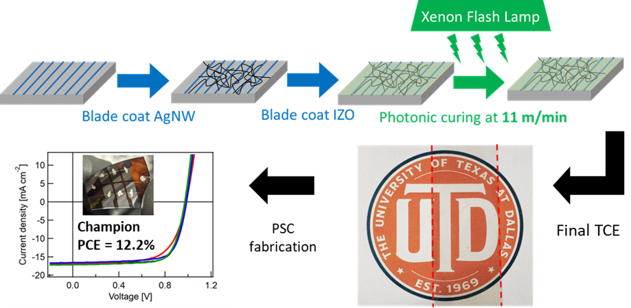
This study presents an innovative material processing approach to fabricate transparent conducting electrodes (TCEs) on polyethylene terephthalate (PET) substrates using blade coating and photonic curing. The hybrid TCEs consist of a multiscale Ag network, combining silver metal bus lines and nanowires, overcoated by an indium zinc oxide layer, and then photonically cured. Blade coating ensures film uniformity and thickness control over large areas. Photonic curing, a non-thermal processing method with significantly lower carbon emissions, enhances the conductivity and transparency of the coated layers. Our hybrid TCEs achieve an average transmittance of (81 ± 0.4)% referenced to air ((90 ± 0.4)% referenced to the PET substrate) in the visible range, an average sheet resistance of (11 ± 0.5) Ω sq−1, and an average surface roughness of (4.3 ± 0.4) nm. We benchmark these values against commercial PET/TCE substrates. Mechanical durability tests demonstrate <3% change in resistance after 2000 bending cycles at a 1 in radius. The scalable potential of the hybrid TCE fabrication method is demonstrated by high uniformity and excellent properties in 7 in × 8 in large-area samples and by performing the photonic curing process at 11 m min−1. Furthermore, halide perovskite solar cells fabricated on these hybrid TCEs achieve average and champion power conversion efficiencies of (10.5 ± 1.0) % and 12.2%, respectively, and significantly outperform devices made on commercial PET/TCEs. This work showcases our approach as a viable pathway for high-speed “green” manufacturing of high-performance TCEs on PET substrates for flexible optoelectronic devices.
- Open Access
- Article
“Green” Fabrication of High-performance Transparent Conducting Electrodes by Blade Coating and Photonic Curing on PET for Perovskite Solar Cells
- Justin C. Bonner 1, †,
- Robert T. Piper 1, †,
- Bishal Bhandari 2,
- Cody R. Allen 2,
- Cynthia T. Bower 3, 4,
- Melinda A. Ostendorf 3, 4,
- Matthew Davis 5,
- Marisol Valdez 6,
- Mark Lee 2,
- Julia W. P. Hsu 1, ∗
Author Information
Received: 30 Sep 2024 | Revised: 25 Oct 2024 | Accepted: 30 Oct 2024 | Published: 05 Nov 2024
Abstract
Graphical Abstract
Keywords
transparent conducting electrode | photonic curing | roll-to-roll | silver nanowires | blade-coating | “green” manufacturing
References
- 1.Nguyen, V.H.; Papanastasiou, D.T.; Resende, J.; Bardet, L.; Sannicolo, T.; Jiménez, C.; Muñoz-Rojas, D.; Nguyen, N.D.; Bellet, D. Advances in Flexible Metallic Transparent Electrodes. Small 2022, 18, 2106006. https://doi.org/10.1002/smll.202106006.
- 2.McLellan, K.; Yoon, Y.; Leung, S.N.; Ko, S.H. Recent Progress in Transparent Conductors Based on Nanomaterials: Advancements and Challenges. Adv. Mater. Technol. 2020, 5, 1900939. https://doi.org/10.1002/admt.201900939.
- 3.Ellmer, K. Past Achievements and Future Challenges in the Development of Optically Transparent Electrodes. Nat. Photonics 2012, 6, 809–817. https://doi.org/10.1038/nphoton.2012.282.
- 4.Zhang, Y.; Ng, S.W.; Lu, X.; Zheng, Z. Solution-Processed Transparent Electrodes for Emerging Thin-Film Solar Cells. Chem. Rev. 2020, 120, 2049–2122. https://doi.org/10.1021/acs.chemrev.9b00483.
- 5.Lee, M.; Piper, R.T.; Bhandari, B.; Hsu, J.W.P. Multiobjective Optimization of Silver-Nanowire Deposition for Flexible Transparent Conducting Electrodes. ACS Appl. Nano Mater. 2023, 6, 17364–17368. https://doi.org/10.1021/acsanm.3c03599.
- 6.Sigma, M. Indium Tin Oxide Coated PET Available online: https://www.sigmaaldrich.com/US/en/product/aldrich/639303 (accessed on 1 June 2023).
- 7.Laghrib, S.; Benhaliliba, M.; Adnani, H.; Abdi, D. Wide Bandgap Indium-Doped SnO2 Semiconductor Prepared by Sol-Gel Route: Multilayer Fabrication and Low Resistivity for Solar Cell Application. J. Sol-Gel Sci. Technol. 2023, 106, 530–544. https://doi.org/10.1007/s10971-023-06093-y.
- 8.Fan, X. Doping and Design of Flexible Transparent Electrodes for High-Performance Flexible Organic Solar Cells: Recent Advances and Perspectives. Adv. Funct. Mater. 2021, 31, 2009399. https://doi.org/10.1002/adfm.202009399.
- 9.Lu, X.; Zhang, Y.; Zheng, Z. Metal-Based Flexible Transparent Electrodes: Challenges and Recent Advances. Adv. Electron. Mater. 2021, 7, 2001121. https://doi.org/10.1002/aelm.202001121.
- 10.Lee, H.B.; Jin, W.Y.; Ovhal, M.M.; Kumar, N.; Kang, J.W. Flexible Transparent Conducting Electrodes Based on Metal Meshes for Organic Optoelectronic Device Applications: A Review. J. Mater. Chem. C 2019, 7, 1087–1110. https://doi.org/10.1039/c8tc04423f.
- 11.Azani, M.; Hassanpour, A.; Torres, T. Benefits, Problems, and Solutions of Silver Nanowire Transparent Conductive Electrodes in Indium Tin Oxide (ITO)-Free Flexible Solar Cells. Adv. Energy Mater. 2020, 10, 2002536. https://doi.org/10.1002/aenm.202002536.
- 12.Parente, M.; Van Helvert, M.; Hamans, R.F.; Verbroekken, R.; Sinha, R.; Bieberle-Hütter, A.; Baldi, A. Simple and Fast High-Yield Synthesis of Silver Nanowires. Nano Lett. 2020, 20, 5759–5764. https://doi.org/10.1021/acs.nanolett.0c01565.
- 13.Energy, U.D. of Energy Earthshots—U.S. Department of Energy Industrial Heat Shot. Available online: https://www.energy.gov/sites/default/files/2022-09/earth-shot-industrial-heat-fact-sheet.pdf (accessed on 24 September 2024).
- 14.Schroder, K.A. Mechanisms of Photonic CuringTM: Processing High Temperature Films on Low Temperature Substrates. In Proceedings of the Technical Proceedings of the 2011 NSTI Nanotechnology Conference and Expo, Boca Raton, FL, USA, 13–16 June 2011; pp. 220–223.
- 15.Schroder, K.A.; Martin, K.M.; Jackson, D.K.; McCool, S.C. Method and Apparatus for Curing Thin Films on Low-Temperature Substrates at High Speeds 2013. U.S. Patent 9, 095, 874 B2, 4 August 2014.
- 16.Gerlein, L.F.; Benavides-Guerrero, J.A.; Cloutier, S.G. High-Performance Silver Nanowires Transparent Conductive Electrodes Fabricated Using Manufacturing-Ready High-Speed Photonic Sinterization Solutions. Sci. Rep. 2021, 11, 24156. https://doi.org/10.1038/s41598-021-03528-w.
- 17.Piper, R.T.; Xu, W.; Hsu, J.W.P. Silver Nanowire-Indium Zinc Oxide Composite Flexible Transparent Conducting Electrodes Made by Spin-Coating and Photonic Curing. MRS Adv. 2023, 8, 177–182. https://doi.org/10.1557/s43580-022-00478-x.
- 18.Jiu, J.; Nogi, M.; Sugahara, T.; Tokuno, T.; Araki, T.; Komoda, N.; Suganuma, K.; Uchida, H.; Shinozaki, K. Strongly Adhesive and Flexible Transparent Silver Nanowire Conductive Films Fabricated with a High-Intensity Pulsed Light Technique. J. Mater. Chem. 2012, 22, 23561–23567. https://doi.org/10.1039/c2jm35545k.
- 19.Kim, K.S.; Choi, S.B.; Kim, D.U.; Lee, C.R.; Kim, J.W. Photo-Induced Healing of Stretchable Transparent Electrodes Based on Thermoplastic Polyurethane with Embedded Metallic Nanowires. J. Mater. Chem. A 2018, 6, 12420–12429. https://doi.org/10.1039/c8ta02979b.
- 20.Yang, Y.; Ding, S.; Araki, T.; Jiu, J.; Sugahara, T.; Wang, J.; Vanfleteren, J.; Sekitani, T.; Suganuma, K. Facile Fabrication of Stretchable Ag Nanowire/Polyurethane Electrodes Using High Intensity Pulsed Light. Nano Res. 2016, 9, 401–414. https://doi.org/10.1007/s12274-015-0921-9.
- 21.Schroder, K.A.; McCool, S.C.; Furlan, W.F. Broadcast Photonic Curing of Metallic Nanoparticle Films. In Proceedings of the 2006 NSTI Nanotechnology Conference and Trade Show, Boston, MA, USA, 7–11 May 2006.
- 22.Akhavan, V.; Schroder, K.; Farnsworth, S. Photonic Curing Enabling High-Speed Sintering of Metal Inkjet Inks on Temperature-Sensitive Substrates. In Handbook of Industrial Inkjet Printing; Wiley: Weinheim, Germany, 2017; Volume 2, pp. 557–566, ISBN 9783527687169.
- 23.Galagan, Y.; Coenen, E.W.C.; Abbel, R.; Van Lammeren, T.J.; Sabik, S.; Barink, M.; Meinders, E.R.; Andriessen, R.; Blom, P.W.M. Photonic Sintering of Inkjet Printed Current Collecting Grids for Organic Solar Cell Applications. Org. Electron. 2013, 14, 38–46. https://doi.org/10.1016/j.orgel.2012.10.012.
- 24.Ghahremani, A.H.; Pishgar, S.; Bahadur, J.; Druffel, T. Intense Pulse Light Annealing of Perovskite Photovoltaics Using Gradient Flashes. ACS Appl. Energy Mater. 2020, 3, 11641–11654. https://doi.org/10.1021/acsaem.0c01520.
- 25.Lavery, B.W.; Kumari, S.; Konermann, H.; Draper, G.L.; Spurgeon, J.; Druffel, T. Intense Pulsed Light Sintering of CH3NH3PbI3 Solar Cells. ACS Appl. Mater. Interfaces 2016, 8, 8419–8426. https://doi.org/10.1021/acsami.5b10166.
- 26.Xu, W.; Daunis, T.B.; Piper, R.T.; Hsu, J.W.P. Effects of Photonic Curing Processing Conditions on MAPbI 3 Film Properties and Solar Cell Performance. ACS Appl. Energy Mater. 2020, 3, 8636–8645. https://doi.org/10.1021/acsaem.0c01243.
- 27.Piper, R.T.; Daunis, T.B.; Xu, W.; Schroder, K.A.; Hsu, J.W.P. Photonic Curing of Nickel Oxide Transport Layer and Perovskite Active Layer for Flexible Perovskite Solar Cells: A Path Towards High-Throughput Manufacturing. Front. Energy Res. 2021, 9, 76. https://doi.org/10.3389/fenrg.2021.640960.
- 28.Troughton, J.; Carnie, M.J.; Davies, M.L.; Charbonneau, C.; Jewell, E.H.; Worsley, D.A.; Watson, T.M. Photonic Flash-Annealing of Lead Halide Perovskite Solar Cells in 1 Ms. J. Mater. Chem. A 2016, 4, 3471–3476. https://doi.org/10.1039/c5ta09431c.
- 29.Piper, R.T.; Xu, W.; Hsu, J.W.P. How Optical and Electrical Properties of ITO Coated Willow Glass Affect Photonic Curing Outcome for Upscaling Perovskite Solar Cell Manufacturing. IEEE J. Photovolt. 2022, 12, 722–727. https://doi.org/10.1109/JPHOTOV.2022.3159395.
- 30.Das, S.; Gu, G.; Joshi, P.C.; Yang, B.; Aytug, T.; Rouleau, C.M.; Geohegan, D.B.; Xiao, K. Low Thermal Budget, Photonic-Cured Compact TiO2 Layers for High-Efficiency Perovskite Solar Cells. J. Mater. Chem. A 2016, 4, 9685–9690. https://doi.org/10.1039/c6ta02105k.
- 31.Daunis, T.B.; Schroder, K.A.; Hsu, J.W.P. Photonic Curing of Solution-Deposited ZrO2 Dielectric on PEN: A Path towards High-Throughput Processing of Oxide Electronics. NPJ Flex. Electron. 2020, 4, 7. https://doi.org/10.1038/s41528-020-0070-4.
- 32.Ghahremani, A.H.; Martin, B.; Gupta, A.; Bahadur, J.; Ankireddy, K.; Druffel, T. Rapid Fabrication of Perovskite Solar Cells through Intense Pulse Light Annealing of SnO2 and Triple Cation Perovskite Thin Films. Mater. Des. 2020, 185, 108237. https://doi.org/10.1016/j.matdes.2019.108237.
- 33.Feleki, B.; Bex, G.; Andriessen, R.; Galagan, Y.; Di Giacomo, F. Rapid and Low Temperature Processing of Mesoporous TiO2 for Perovskite Solar Cells on Flexible and Rigid Substrates. Mater. Today Commun. 2017, 13, 232–240. https://doi.org/10.1016/j.mtcomm.2017.09.007.
- 34.Martin, B.; Amos, D.; Brehob, E.; van Hest, M.F.A.M.; Druffel, T. Techno-Economic Analysis of Roll-to-Roll Production of Perovskite Modules Using Radiation Thermal Processes. Appl. Energy 2022, 307, 118200. https://doi.org/10.1016/j.apenergy.2021.118200.
- 35.Scheideler, W.J.; Smith, J.; Deckman, I.; Chung, S.; Arias, A.C.; Subramanian, V. A Robust, Gravure-Printed, Silver Nanowire/Metal Oxide Hybrid Electrode for High-Throughput Patterned Transparent Conductors. J. Mater. Chem. C 2016, 4, 3248–3255. https://doi.org/10.1039/C5TC04364F.
- 36.Lee, E.; Ahn, J.; Kwon, H.C.; Ma, S.; Kim, K.; Yun, S.; Moon, J. All-Solution-Processed Silver Nanowire Window Electrode-Based Flexible Perovskite Solar Cells Enabled with Amorphous Metal Oxide Protection. Adv. Energy Mater. 2018, 8, 1702182. https://doi.org/10.1002/aenm.201702182.
- 37.Kim, S.; Kim, S.Y.; Kim, J.; Kim, J.H. Highly Reliable AgNW/PEDOT:PSS Hybrid Films: Efficient Methods for Enhancing Transparency and Lowering Resistance and Haziness. J. Mater. Chem. C 2014, 2, 5636–5643. https://doi.org/10.1039/c4tc00686k.
- 38.Morgenstern, F.S.F.; Kabra, D.; Massip, S.; Brenner, T.J.K.; Lyons, P.E.; Coleman, J.N.; Friend, R.H. Ag-Nanowire Films Coated with ZnO Nanoparticles as a Transparent Electrode for Solar Cells. Appl. Phys. Lett. 2011, 99, 183307. https://doi.org/10.1063/1.3656973.
- 39.Wu, C.; Jiu, J.; Araki, T.; Koga, H.; Sekitani, T.; Wang, H.; Suganuma, K. Rapid Self-Assembly of Ultrathin Graphene Oxide Film and Application to Silver Nanowire Flexible Transparent Electrodes. RSC Adv. 2016, 6, 15838–15845. https://doi.org/10.1039/c5ra24896e.
- 40.Lee, J.Y.; Connor, S.T.; Cui, Y.; Peumans, P. Solution-Processed Metal Nanowire Mesh Transparent Electrodes. Nano Lett. 2008, 8, 689–692. https://doi.org/10.1021/nl073296g.
- 41.Lu, H.; Sun, J.; Zhang, H.; Lu, S.; Choy, W.C.H.H. Room-Temperature Solution-Processed and Metal Oxide-Free Nano-Composite for the Flexible Transparent Bottom Electrode of Perovskite Solar Cells. Nanoscale 2016, 8, 5946–5953. https://doi.org/10.1039/C6NR00011H.
- 42.Chen, X.; Xu, G.; Zeng, G.; Gu, H.; Chen, H.; Xu, H.; Yao, H.; Li, Y.; Hou, J.; Li, Y. Realizing Ultrahigh Mechanical Flexibility and >15% Efficiency of Flexible Organic Solar Cells via a “Welding” Flexible Transparent Electrode. Adv. Mater. 2020, 32, 1908478. https://doi.org/10.1002/adma.201908478.
- 43.He, W.W.; Yan, X.H.; Liang, Y.M.; Long, Y.F.; Pan, C.; Zhao, J.L.; Chen, L.; Xiong, W.; Liu, Q.X. Scalable and Cost-Effective Ag Nanowires Flexible Transparent Electrodes. RSC Adv. 2018, 8, 12146–12151. https://doi.org/10.1039/c7ra13196h.
- 44.Kim, M.G.; Kanatzidis, M.G.; Facchetti, A.; Marks, T.J. Low-Temperature Fabrication of High-Performance Metal Oxide Thin-Film Electronics via Combustion Processing. Nat. Mater. 2011, 10, 382–388. https://doi.org/10.1038/nmat3011.
- 45.Lee, S.H.; Hong, S.; Kim, H.J. Selection of a Suitable Solvent Additive for 2-Methoxyethanol-Based Antisolvent-Free Perovskite Film Fabrication. ACS Appl. Mater. Interfaces 2022, 14, 39132–39140. https://doi.org/10.1021/acsami.2c10171.
- 46.Park, S.; Kim, K.; Jo, J.; Sung, S.; Kim, K.; Lee, W.; Kim, J.; Kim, H.J.; Yi, G.; Kim, Y.; et al. In-Depth Studies on Rapid Photochemical Activation of Various Sol–Gel Metal Oxide Films for Flexible Transparent Electronics. Adv. Funct. Mater. 2015, 25, 2807–2815. https://doi.org/10.1002/adfm.201500545.
- 47.Kim, H.J.; Jung, J.; Kim, H.J. Enhancement of Electrical Characteristics and Stability of Self-Patterned In–Zn–O Thin-Film Transistors Based on Photosensitive Precursors. Sci. Rep. 2020, 10, 18853. https://doi.org/10.1038/s41598-020-76080-8.
- 48.Baltrusaitis, J.; Jayaweera, P.M.; Grassian, V.H. XPS Study of Nitrogen Dioxide Adsorption on Metal Oxide Particle Surfaces under Different Environmental Conditions. Phys. Chem. Chem. Phys. 2009, 11, 8295–8305. https://doi.org/10.1039/b907584d.
- 49.Anand, A.; Islam, M.M.; Meitzner, R.; Schubert, U.S.; Hoppe, H. Introduction of a Novel Figure of Merit for the Assessment of Transparent Conductive Electrodes in Photovoltaics: Exact and Approximate Form. Adv. Energy Mater. 2021, 11, 2100875. https://doi.org/10.1002/aenm.202100875.
- 50.De, S.; King, P.J.; Lyons, P.E.; Khan, U.; Coleman, J.N. Size Effects and the Problem with Percolation in Nanostructured Transparent Conductors. ACS Nano 2010, 4, 7064–7072. https://doi.org/10.1021/nn1025803.
- 51.Dressel George, M.G. Electrodynamics of Solids; Cambridge University Press: Cambridge, 2002; ISBN 9780511606168.
- 52.Optical Filters. USA LCC Optical Filters. Available online: https://www.opticalfiltersusa.com/ (accessed on 1 June 2023).
- 53.Gower, J.C. Generalized Procrustes Analysis. Psychometrika 1975, 40, 33–51. https://doi.org/10.1007/BF02291478.
- 54.Bhandari, B.; Bonner, J.C.; Piper, R.T.; Hsu, J.W.P. Effects of Transparent Conducting Electrodes and Hole Transport Layers on the Performance of MAPbI 3 Solar Cells Fabricated on PET Substrates. Flex. Print. Electron. 2024, 9, 035002. https://doi.org/10.1088/2058-8585/ad5d01.
- 55.Kim, S.Y.; Cho, S.J.; Byeon, S.E.; He, X.; Yoon, H.J. Self-Assembled Monolayers as Interface Engineering Nanomaterials in Perovskite Solar Cells. Adv. Energy Mater. 2020, 10, 2002606. https://doi.org/10.1002/aenm.202002606.
- 56.Ali, F.; Roldán-Carmona, C.; Sohail, M.; Nazeeruddin, M.K. Applications of Self-Assembled Monolayers for Perovskite Solar Cells Interface Engineering to Address Efficiency and Stability. Adv. Energy Mater. 2020, 10, 2002989. https://doi.org/10.1002/aenm.202002989.
How to Cite
Bonner, J. C.; Piper, R. T.; Bhandari, B.; Allen, C. R.; Bower, C. T.; Ostendorf, M. A.; Davis, M.; Valdez, M.; Lee, M.; Hsu, J. W. P. “Green” Fabrication of High-performance Transparent Conducting Electrodes by Blade Coating and Photonic Curing on PET for Perovskite Solar Cells. Materials and Sustainability 2025, 1 (1), 2. https://doi.org/10.53941/matsus.2025.100002.
RIS
BibTex
Copyright & License

Copyright (c) 2025 by the authors.
This work is licensed under a Creative Commons Attribution 4.0 International License.
Contents
References
 Suite 4002 Level 4, 447 Collins Street, Melbourne, Victoria 3000, Australia
 General Inquiries: info@sciltp.com